Semiconductors are materials with a bandgap and variable electronic conductivity used as the core component of optoelectronic devices. Several classes of semiconductors are distinguished by nature of participating electrons, see these slides.
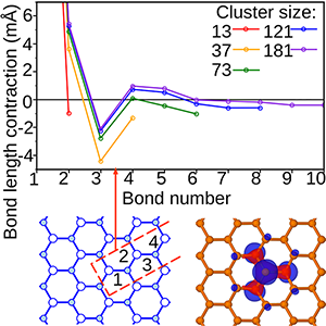
Several electronically different classes of two-dimensional (2D) semiconductors are well known nowadays including graphene family, transition metal dichalcogenides, and pnictogens. Many of their unique properties remain poorely understood calling for in-depth theoretical study.

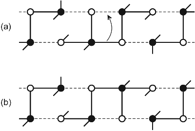
Amorphous pnictide and chalcogenide semiconductors (As, Se, As2Se3, Ge2Sb2Te5 etc., see the diagram and Library) exhibit significant photo- and current-induced changes whose nature is not well understood thus limiting the potential applications of the phenomenon (see for example phase-change memory).

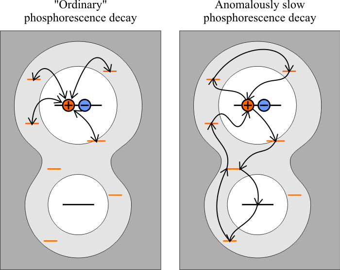
Nanostructured silicon (porous-Si, Si nanocrystals in SiO2, Si nanowires etc., see the Library) raised a wave of scientific activity in 1990 as the promising material for silicon based optoelectronics. The kinetics of the phosphorescence decay of a porous silicon in a wide temperature range is anomalously slow (the integral over the extrapolated signal diverges). This phenomena is observed in some conjugated polymers, but the existing explanation as the tunneling recombination of geminate electron-hole pairs requires an unnatural distribution of activation energies for porous silicon: wide, flat, with depression at small energies.
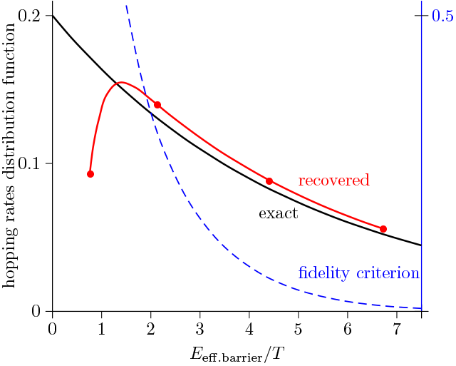
The analysis of the luminescence response is one of the easiest tools for studying the physical properties of materials. In particular, much information can be obtained by deconvoluting the time curve of the luminescence decay. The deconvolution is nontrivial, except the case of the multi-exponential decay, since the numerical inverse-Laplace transformation is mathematically incorrect problem.
